One thing that all schematics have in common is the utter inability to drive a motor, or blink an LED, or filter out noise, or do any of the other useful and interesting things that we expect electrical systems to do. A schematic is, after all, just a drawing. To actually accomplish something with a circuit, we need to translate its schematic into physical components and physical interconnections. Simple schematics can often be realized on a breadboard, but the vast majority of circuit designs enter the physical realm in the form of a printed circuit board, or PCB for short.
The Structure of a PCB
A very basic printed circuit board is a flat, rigid, insulating material that has thin conductive structures adhering to one side. These conductive structures create geometric patterns consisting of, for example, rectangles, circles, and squares. Long, thin rectangles function as interconnections (i.e., the equivalent of wires), and various shapes function as connection points for components.

This is an example of a very basic PCB. This board is actually homemade; see AAC’s guide to home PCB fabrication for more information.
A printed circuit board such as the example in the image has only one conductive layer. A single-layer PCB is very restrictive; the circuit realization will not make efficient use of available area, and the designer may have difficulty creating the necessary interconnections.
Incorporating additional conductive layers makes the PCB more compact and easier to design. A two-layer board is a major improvement over a single-layer board, and most applications benefit from having at least four layers. A four-layer board consists of the top layer, the bottom layer, and two internal layers. (“Top” and “bottom” may not seem like typical scientific terminology, but they are nonetheless the official designations in the world of PCB design and fabrication.)
PCB Stackup
The stackup is the arrangement of conductive and insulating layers in a multilayer PCB. The following side-view diagram shows the stackup of a four-layer board.
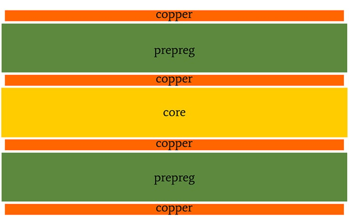
The conductive material of choice is copper. Prepreg is an insulating material that is pre-impregnated (hence the name) with resin, and the core (also insulating) is similar in composition to the prepreg.
I recommend that you use a four-layer structure whenever possible. A four-layer board allows you to devote one internal layer to the reference potential (i.e., ground) and another internal layer to power-supply voltages. The top, and if necessary the bottom, will be a component layer. This arrangement facilitates PCB design and also helps you to achieve improved circuit performance.
Understanding PCB Features and Terminology
There’s quite a bit of specialized vocabulary that arises in discussions of printed circuit boards. This section describes physical structures found on PCBs and gives you the words that we use to identify them.
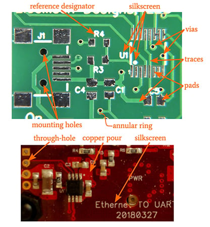
A conductive interconnection is called a trace, and connection points for components are called pads (for pins that rest on the surface of the board) and through-holes (for pins that are inserted into holes drilled in the board). Basic PCB design consists of arranging pads and through-holes so that components can be properly installed, and then connecting these pads and through-holes using traces.
Not all drilled holes are for through-hole components. We often need to transfer a signal or supply voltage from one PCB layer to another, and this is accomplished using small, conductive holes called vias.
Many PCBs also include mounting holes, which have a mechanical rather than an electrical function and therefore don’t need to be plated. The term “plating” in this context refers to conductive material that has been deposited onto the interior of a drilled hole.
A copper pour is a relatively large section of a PCB layer that is filled with conductive material. Copper pours can be used to provide a very low-resistance or low-inductance connection between components and to improve thermal performance.
A PCB layer that consists entirely of one large copper pour is called a plane layer. We frequently use an internal layer as a ground plane and create ground connections by placing vias next to component pins.
A through-hole or via begins as a circle of copper and then becomes a hole when a drill bit passes through the circle (ideally through the center of the circle). The term annular ring refers to the width of copper that remains after the hole has been drilled.
Printed circuit boards include a variety of “supplemental” information that have no role in the electrical functionality of the device. For example, reference designators uniquely identify components, dots indicate proper component orientation, and project titles or serial numbers help us to keep track of the many circuit boards that accumulate in a lab. We refer to this information as the silkscreen.
For more electronic components requirements,pls see:https://www.megasourceel.com/products.html